Flash PCIe cables – Models 982, 98F (All Flash)
These tables show the point-to-point connections for Flash PCIe cables on a Model 982, with or without expansion racks. Flash enclosures that are shown here are HPFE (Gen1). For flash PCIe and SAS configurations with HPFE Gen2, refer to Flash PCIe and SAS cables – Models 982, 98F with HPFE Gen2.
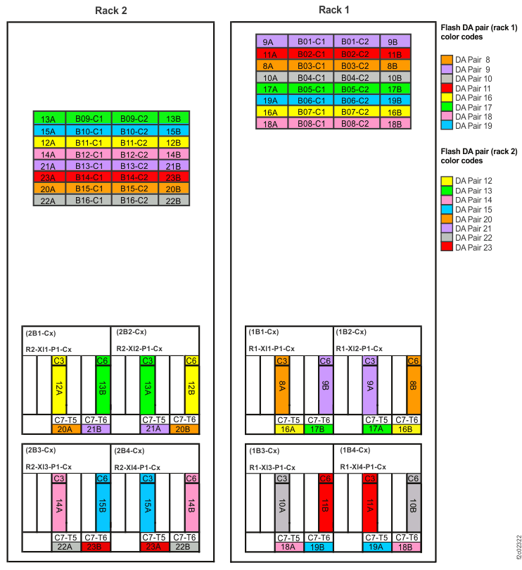
- Racks are shown with the maximum number of storage enclosures and device adapter cards. Your rack might contain fewer storage enclosures or device adapter cards.
- Figure 1 shows the maximum number of racks in a storage facility with these rack models.
Flash PCIe Cables
- Flash PCIe cables and connectors are identified with a colored band matching the DA pair and two
different color codes:
- A colored band, corresponding to the color code of the DA pair, is found on each end of the cable near the connector. These color codes are shown in Figure 1.
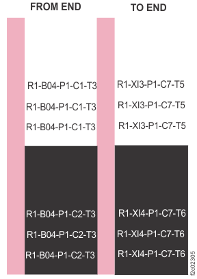
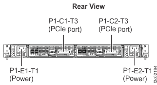
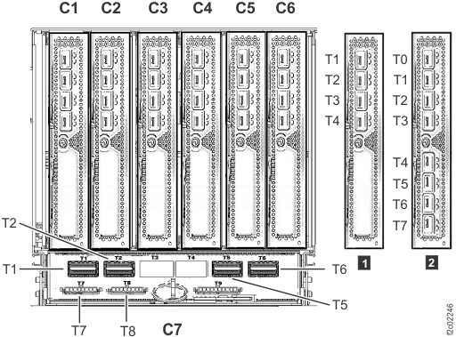
- The connector is color-coded to help prevent cross-cabling at the RAID controller card or I/O enclosure PCIe and PCN card end. Connectors on cables attaching to Rx-Bxx-P1-C1-T3 have white labels with black text, and connectors on cables attaching to Rx-Bxx-P1-C2-T3 have black labels with white text. An example of this showing both cables attaching to an enclosure is shown in Figure 2. This alternating color scheme is the same for all Flash PCIe cables, and is independent of the DA pair color code. Figure 3 and Figure 4 show the Flash PCIe cable connection points.
- The black and white label at each end has a physical location code showing the "FROM" and "TO" end.
- If the cable connects to an I/O enclosure device adapter card connector, the physical location code is similar to this example: R1-XI3-P1-C7-T5. Refer to I/O enclosure location codes (Models 98x) (not 983).
- If the cable connects to a storage enclosure RAID controller card, the physical location code is similar to this example: R1-B04-P1-C1-T3. Refer to Storage enclosure location codes (Models 98x, PCIe flash enclosure, 30 SSD slots, 1.8 inches).
Flash PCIe cabling tables
Table 1 and Table 2 show a summary of Flash PCIe cabling for models 982 and 98F.
Table 3 shows details of the Flash PCIe cabling with Rack 1 high-performance flash enclosures (device adapter pairs 8, 9, 10, 11, 16, 17, 18, and 19, in normal installation order).
Table 4 shows details of the Flash PCIe cabling with Rack 2 high-performance flash enclosures (device adapter pairs 12, 13, 14, 15, 20, 21, 22, and 23, in normal installation order).
Note: Location designators are labeled as link in the following tables.
| From DA pair | DA pair (link) | To storage enclosure |
|---|---|---|
| R1-XI3-P1-C7-T5 R1-XI4-P1-C7-T6 |
18(A) 18(B) |
R1-B08 |
| R1-XI1-P1-C7-T5 R1-XI2-P1-C7-T6 |
16(A) 16(B) |
R1-B07 |
| R1-XI4-P1-C7-T5 R1-XI3-P1-C7-T6 |
19(A) 19(B) |
R1-B06 |
| R1-XI2-P1-C7-T5 R1-XI1-P1-C7-T6 |
17(A) 17(B) |
R1-B05 |
| R1-XI3-P1-C3-T1 R1-XI4-P1-C6-T1 |
10(A) 10(B) |
R1-B04 |
| R1-XI1-P1-C3-T1 R1-XI2-P1-C6-T1 |
8 (A) 8 (B) |
R1-B03 |
| R1-XI4-P1-C3-T1 R1-XI3-P1-C6-T1 |
11(A) 11(B) |
R1-B02 |
| R1-XI2-P1-C3-T1 R1-XI1-P1-C6-T1 |
9 (A) 9 (B) |
R1-B01 |
| From DA pair | DA pair (link) | To storage enclosure |
|---|---|---|
| R2-XI3-P1-C7-T5 R2-XI4-P1-C7-T6 |
22(A) 22(B) |
R2-B16 |
| R2-XI1-P1-C7-T5 R2-XI2-P1-C7-T6 |
20(A) 20(B) |
R2-B15 |
| R2-XI4-P1-C7-T5 R2-XI3-P1-C7-T6 |
23(A) 23(B) |
R2-B14 |
| R2-XI2-P1-C7-T5 R2-XI1-P1-C7-T6 |
21(A) 21(B) |
R2-B13 |
| R2-XI3-P1-C3-T1 R2-XI4-P1-C6-T1 |
14(A) 14(B) |
R2-B12 |
| R2-XI1-P1-C3-T1 R2-XI2-P1-C6-T1 |
12(A) 12(B) |
R2-B11 |
| R2-XI4-P1-C3-T1 R2-XI3-P1-C6-T1 |
15(A) 15(B) |
R2-B10 |
| R2-XI2-P1-C3-T1 R2-XI1-P1-C6-T1 |
13(A) 13(B) |
R2-B09 |
| From DA | Link | To RAID controller card |
|---|---|---|
| R1-XI3-P1-C7-T5 | 18A | R1-B08-P1-C1-T3 |
| R1-XI4-P1-C7-T6 | 18B | R1-B08-P1-C2-T3 |
| R1-XI1-P1-C7-T5 | 16A | R1-B07-P1-C1-T3 |
| R1-XI2-P1-C7-T6 | 16B | R1-B07-P1-C2-T3 |
| R1-XI4-P1-C7-T5 | 19A | R1-B06-P1-C1-T3 |
| R1-XI3-P1-C7-T6 | 19B | R1-B06-P1-C2-T3 |
| R1-XI2-P1-C7-T5 | 17A | R1-B05-P1-C1-T3 |
| R1-XI1-P1-C7-T6 | 17B | R1-B05-P1-C2-T3 |
| R1-XI3-P1-C3-T1 | 10A | R1-B04-P1-C1-T3 |
| R1-XI4-P1-C6-T1 | 10B | R1-B04-P1-C2-T3 |
| R1-XI1-P1-C3-T1 | 8A | R1-B03-P1-C1-T3 |
| R1-XI2-P1-C6-T1 | 8B | R1-B03-P1-C2-T3 |
| R1-XI4-P1-C3-T1 | 11A | R1-B02-P1-C1-T3 |
| R1-XI3-P1-C6-T1 | 11B | R1-B02-P1-C2-T3 |
| R1-XI2-P1-C3-T1 | 9A | R1-B01-P1-C1-T3 |
| R1-XI1-P1-C6-T1 | 9B | R1-B01-P1-C2-T3 |
| From DA | Link | To RAID controller card |
|---|---|---|
| R2-XI3-P1-C7-T5 | 22A | R2-B16-P1-C1-T3 |
| R2-XI4-P1-C7-T6 | 22B | R2-B16-P1-C2-T3 |
| R2-XI1-P1-C7-T5 | 20A | R2-B15-P1-C1-T3 |
| R2-XI2-P1-C7-T6 | 20B | R2-B15-P1-C2-T3 |
| R2-XI4-P1-C7-T5 | 23A | R2-B14-P1-C1-T3 |
| R2-XI3-P1-C7-T6 | 23B | R2-B14-P1-C2-T3 |
| R2-XI2-P1-C7-T5 | 21A | R2-B13-P1-C1-T3 |
| R2-XI1-P1-C7-T6 | 21B | R2-B13-P1-C2-T3 |
| R2-XI3-P1-C3-T1 | 14A | R2-B12-P1-C1-T3 |
| R2-XI4-P1-C6-T1 | 14B | R2-B12-P1-C2-T3 |
| R2-XI1-P1-C3-T1 | 12A | R2-B11-P1-C1-T3 |
| R2-XI2-P1-C6-T1 | 12B | R2-B11-P1-C2-T3 |
| R2-XI4-P1-C3-T1 | 15A | R2-B10-P1-C1-T3 |
| R2-XI3-P1-C6-T1 | 15B | R2-B10-P1-C2-T3 |
| R2-XI2-P1-C3-T1 | 13A | R2-B09-P1-C1-T3 |
| R2-XI1-P1-C6-T1 | 13B | R2-B09-P1-C2-T3 |