Flash PCIe and SAS cables – Models 981, 98E with HPFE Gen2 (three-phase power)
The tables in this topic show the point-to-point connections for flash PCIe
and SAS cables on a Model 981 (three-phase power) with HPFE Gen2, with or without expansion racks.
For FC-AL and flash PCIe configurations with HPFE (Gen1), refer to FC-AL and Flash PCIe cables – Models 981, 98E (three-phase power).
Notes:
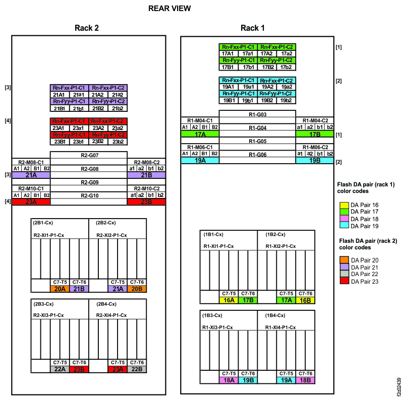
- Racks are shown with the maximum number of HPFE Gen2 storage enclosures and device adapter cards. Your rack might contain fewer storage enclosures or device adapter cards.
- The figures that follow show the maximum number of racks in a storage facility with these rack models.
Notes:
- Only HPFE Gen2 PCIe and SAS details are shown.
- For this model, physical locations are predefined for microbays, but not for HPFE Gen2 flash enclosures.
- The HPFE Gen2 enclosure pair can be located in a different rack than the associated microbay pair.
- The HPFE Gen2 enclosure locations are shown as Rn-Fxx (the upper enclosure of a pair) and Rn-Fyy (the lower enclosure of a pair).
Flash PCIe cables
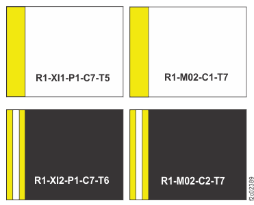
- Flash PCIe cables and connectors are identified with a colored band matching the DA pair and two
different color codes:
- A colored band, corresponding to the color code of the DA pair, is found on each end of the cable near the connector. These color codes are shown in Figure 1.
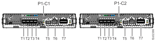
- The connector is color-coded to help prevent cross-cabling at the microbay adapter card or I/O enclosure PCIe and PCN card end. Connectors on cables attaching to Rx-Mxx-C1-T7 have white labels with black text, and connectors on cables attaching to Rx-Mxx-C2-T7 have black labels with white text. An example of this showing both cables attaching to a microbay adapter card pair is shown in Figure 2. This alternating color scheme is the same for all Flash PCIe cables, and is independent of the DA pair color code. Figure 3 and Figure 4 show the Flash PCIe cable connection ends.
- The black and white label at each end has a physical location code showing the "FROM" and "TO" end.
-
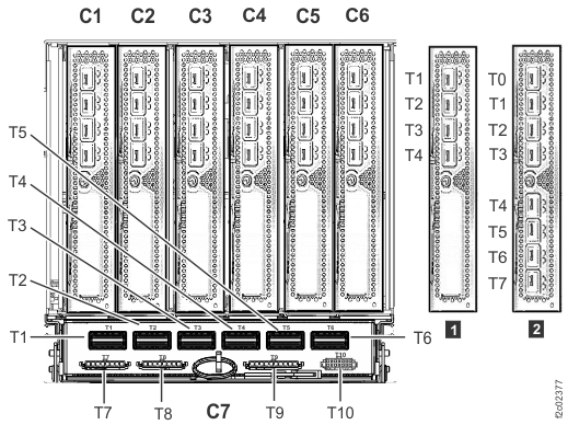
- If the cable connects to an I/O enclosure device adapter card connector, the physical location code is similar to this example: R1-XI1-P1-C7-T5. Refer to I/O enclosure location codes (Models 98x) (not 983).
- If the cable connects to a microbay adapter card, the physical location code is similar to this example: R1-M02-C1-T7. Refer to Storage enclosure location codes (Models 98x, SAS flash enclosure, 24 drive slots, 2.5 inches).
-
Flash SAS cables
- SAS cables and connectors are identified with two different color codes and a location designator:
- A colored band, corresponding to the color code of the DA pair, is found on each end of the cable near the connector. These color codes are shown in Figure 1.
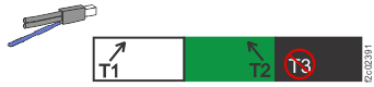
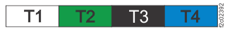
- The connector itself is color coded to help prevent cross-cabling at the SAS expander card or
device adapter card (DA) end. The connectors always appear in the following
order:
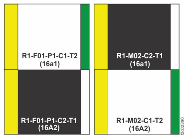
as shown in Figure 6 and Figure 7 . This color code is specific to each SAS expander card or DA, and is independent of the DA pair color code.white (T1), green (T2), black (T3), and blue (T4) - A black or white label at each end of the cable shows a location designator (for example, 16A1). Both ends of the cable have the same location designator and DA pair color code. However, the connector at each end of the same cable usually does NOT have the same color code.
- The following alternating color scheme is the same for all Flash SAS cables, and is independent
of the DA pair color code.
- Connectors on cables that attach to Rx-Mxx-C1-Tx have white labels with black text.
- Connectors on cables that attach to Rx-Mxx-C2-Tx have black labels with white text.
- Connectors on cables that attach to Rx-Mxx-C1-Tx have white labels with black text.
- Connectors on cables that attach to Rx-Mxx-C2-Tx have black labels with white text.
An example of SAS cables and connectors that shows both ends of two SAS cables to an enclosure is shown in Figure 5.
- Location designators are in the form CTP, where:
- C
- Is the device adapter pair (16-23).
- T
- Is the port pair on the device adapter (A, B, a, b) (uppercase for left device adapter in pair, lowercase for right device adapter in pair).
- P
- Is the logical position of the downstream SAS expander card.
Example: 16a1 is the link between device adapter R1-M02-C2-T1 and R1-F01-P1-C1-T2.- 16
- Device adapter pair 16
- a
- First port pair on right adapter of device adapter pair (lowercase a)
- 1
- First SAS expander card
- The black and white label at each end may have a physical location code in addition to
the location designator.
- If the cable connects to a microbay device adapter card connector, the physical location code is similar to this example: R1-M04-C1-T1. Refer to I/O enclosure location codes (Models 98x) (not 983).
- If the cable connects to a storage enclosure SAS expander card, the physical location code is similar to this example: R1-F03-P1-C1-T1. Refer to Storage enclosure location codes (Models 98x, SAS flash enclosure, 24 drive slots, 2.5 inches).
Flash PCIe and SAS cabling tables
Table 1 and
Table 2 show a
summary of Flash PCIe / SAS cabling for models 981 and 98E three-phase power.
Table 4 and
Table 5 show
details of the Flash PCIe / SAS cabling with Rack 1 high-performance flash enclosures Gen2 (device
adapter pairs 17 and 19, in normal installation order).
Table 6 and
Table 7 show
details of the Flash PCIe / SAS cabling with Rack 2 high-performance flash enclosures Gen2 (device
adapter pairs 21 and 23, in normal installation order).
Locations in the following tables are shown in Figure 1.
Note: Location designators are labeled as "link" in the following tables.
| From DA pair | DA pair (link) | To Microbay | To storage enclosure | To storage enclosure |
|---|---|---|---|---|
| R1-XI4-P1-C7-T5 R1-XI3-P1-C7-T6 |
19 (A) 19 (B) |
R1-M06 | Rn-Fxx | Rn-Fyy |
| R1-XI2-P1-C7-T5 R1-XI1-P1-C7-T6 |
17 (A) 17 (B) |
R1-M04 | Rn-Fxx | Rn-Fyy |
| From DA pair | DA pair (link) | To Microbay | To storage enclosure | To storage enclosure |
|---|---|---|---|---|
| R2-XI4-P1-C7-T5 R2-XI3-P1-C7-T6 |
23 (A) 23 (B) |
R2-M10 | Rn-Fxx | Rn-Fyy |
| R2-XI2-P1-C7-T5 R2-XI1-P1-C7-T6 |
21 (A) 21 (B) |
R2-M08 | Rn-Fxx | Rn-Fyy |
| Index (Figure 1) |
For this DA pair | If this HPFE (Gen1) is present, a microbay pair cannot be present on the same DA pair: | If this microbay pair is present, an HPFE (Gen1) cannot be present on the same DA pair: | Notes |
|---|---|---|---|---|
| 1 | 17 | R1-B01 | R1-M04 | Rack-1 can contain R1-B01 or R1-M04, but not both. |
| 2 | 19 | R1-B02 | R1-M06 | Rack-1 can contain R1-B02 or R1-M06, but not both. |
| 3 | 21 | R2-B01 | R2-M08 | Rack-2 can contain R2-B01 or R2-M08, but not both. |
| 4 | 23 | R2-B02 | R2-M10 | Rack-2 can contain R2-B02 or R2-M10, but not both. |
| From DA | Link | To microbay |
From: Microbay |
Link |
To: Flash enclosure |
|---|---|---|---|---|---|
| See index 2 Figure 1 | |||||
| R1-XI4-P1-C7-T5 | 19A | R1-M06-C1-T7 | R1-M06-C1-T1 | 19A1 | Rn-Fxx-P1-C1-T1 |
| R1-M06-C2-T1 | 19a1 | Rn-Fxx-P1-C1-T2 | |||
| R1-M06-C1-T2 | 19A2 | Rn-Fxx-P1-C2-T1 | |||
| R1-M06-C2-T2 | 19a2 | Rn-Fxx-P1-C2-T2 | |||
| R1-XI3-P1-C7-T6 | 19B | R1-M06-C2-T7 | R1-M06-C1-T3 | 19B1 | Rn-Fyy-P1-C1-T1 |
| R1-M06-C2-T3 | 19b1 | Rn-Fyy-P1-C1-T2 | |||
| R1-M06-C1-T4 | 19B2 | Rn-Fyy-P1-C2-T1 | |||
| R1-M06-C2-T4 | 19b2 | Rn-Fyy-P1-C2-T2 | |||
| From DA | Link | To microbay |
From: Microbay |
Link |
To: Flash enclosure |
|---|---|---|---|---|---|
| See index 1 in Figure 1 | |||||
| R1-XI2-P1-C7-T5 | 17A | R1-M04-C1-T7 | R1-M04-C1-T1 | 17A1 | Rn-Fxx-P1-C1-T1 |
| R1-M04-C2-T1 | 17a1 | Rn-Fxx-P1-C1-T2 | |||
| R1-M04-C1-T2 | 17A2 | Rn-Fxx-P1-C2-T1 | |||
| R1-M04-C2-T2 | 17a2 | Rn-Fxx-P1-C2-T2 | |||
| R1-XI1-P1-C7-T6 | 17B | R1-M04-C2-T7 | R1-M04-C1-T3 | 17B1 | Rn-Fyy-P1-C1-T1 |
| R1-M04-C2-T3 | 17b1 | Rn-Fyy-P1-C1-T2 | |||
| R1-M04-C1-T4 | 17B2 | Rn-Fyy-P1-C2-T1 | |||
| R1-M04-C2-T4 | 17b2 | Rn-Fyy-P1-C2-T2 | |||
| From DA | Link | To microbay |
From: Microbay |
Link |
To: Flash enclosure |
|---|---|---|---|---|---|
| See index 4 Figure 1 | |||||
| R2-XI4-P1-C7-T5 | 23A | R2-M10-C1-T7 | R2-M10-C1-T1 | 23A1 | Rn-Fxx-P1-C1-T1 |
| R2-M10-C2-T1 | 23a1 | Rn-Fxx-P1-C1-T2 | |||
| R2-M10-C1-T2 | 23A2 | Rn-Fxx-P1-C2-T1 | |||
| R2-M10-C2-T2 | 23a2 | Rn-Fxx-P1-C2-T2 | |||
| R2-XI3-P1-C7-T6 | 23B | R2-M10-C2-T7 | R2-M10-C1-T3 | 23B1 | Rn-Fyy-P1-C1-T1 |
| R2-M10-C2-T3 | 23b1 | Rn-Fyy-P1-C1-T2 | |||
| R2-M10-C1-T4 | 23B2 | Rn-Fyy-P1-C2-T1 | |||
| R2-M10-C2-T4 | 23b2 | Rn-Fyy-P1-C2-T2 | |||
| From DA | Link | To microbay |
From: Microbay |
Link |
To: Flash enclosure |
|---|---|---|---|---|---|
| See index 3 in Figure 1 | |||||
| R2-XI2-P1-C7-T5 | 21A | R2-M08-C1-T7 | R2-M08-C1-T1 | 21A1 | Rn-Fxx-P1-C1-T1 |
| R2-M08-C2-T1 | 21a1 | Rn-Fxx-P1-C1-T2 | |||
| R2-M08-C1-T2 | 21A2 | Rn-Fxx-P1-C2-T1 | |||
| R2-M08-C2-T2 | 21a2 | Rn-Fxx-P1-C2-T2 | |||
| R2-XI1-P1-C7-T6 | 21B | R2-M08-C2-T7 | R2-M08-C1-T3 | 21B1 | Rn-Fyy-P1-C1-T1 |
| R2-M08-C2-T3 | 21b1 | Rn-Fyy-P1-C1-T2 | |||
| R2-M08-C1-T4 | 21B2 | Rn-Fyy-P1-C2-T1 | |||
| R2-M08-C2-T4 | 21b2 | Rn-Fyy-P1-C2-T2 | |||